


 5 / 29

Polymer Congress 2018
Polymer Sciences
ISSN: 2471-9935
Page 25
June 04-05, 2018
London, UK
4
th
Edition of International Conference on
Polymer Science and
Technology
T
he breakthrough of flexible electronics depends upon
suitable large-scale manufacturing routes, likely requiring
very low cost, high-throughput processing techniques. Our
approach to development of organic electronics considered
high-speed roll-to-roll processing routes already employed
industrially. We examined their applicability in creating
transistors and circuits. Central to this is the high-throughput
deposition of polymeric dielectric using a vacuum deposition
route compatible with the preferred processing for molecular
semiconductors, metal contacts and ceramic or other
semiconducting active components. This paper will discuss
the control of dielectric properties as determined by processing
parameters during the thin-film deposition and by the surface
segregation of one component of a monomer mixture to
control interfacial properties of the dielectric. The dielectric
performance will be demonstrated in OTFT devices and circuit
elements.
Recent Publications
1. Abbas G et al. (2013) Hysteresis-free vacuum-
processed acrylate-pentacene organic thin film
transistors. IEEE Electron Device Letters. 34(2):268-
270.
2. Ding Z et al. (2013) Improving the performance of
organic thin film transistors formed on a vacuum
flash-evaporated acrylate insulator. Applied Physics
Letters. 103:233301.
3. Abbas G A W (2014) A high-yielding evaporation-
based process for organic transistors based on
the semiconductor. DNTT. Organic Electronics.
15(9):1998-2006
4. Avila Niño J A (2016) Stable organic static random
access memory from a roll-to-roll compatible vacuum
evaporation process. Organic Electronics. 31:77-81
5. Ding Z et al. (2016) Vacuum production of OTFTs
by vapour jet deposition of dinaphtho[2,3-b:2’,3’-f]
thieno[3,2 b]thiophene (DNTT) on a lauryl acrylate
functionalised dielectric surface. Organic Electronics.
31:90-97.
Biography
Hazel E Assender graduated from the University of Cambridge, followed
with a PhD and two years of Postdoc in the Department of Materials Science
& Metallurgy in Cambridge before moving to an academic post in Oxford
University. She has led a research activity in the Department of Materials,
University of Oxford, UK since 1996 with a focus in the area of thin films
and coatings both of polymer materials or onto polymer substrates. Her
research spans fundamental studies of the thin film and near-surface prop-
erties of polymers, through to materials engineering of thin films and device
structures in large area on polymer substrates. Her particular areas of inter-
est include roll-to-roll deposition, gas barriers, photovoltaics, and transistors/
circuits. Her research has a technology-facing approach bringing underpin-
ning scientific understanding to development of materials and technologies
that integrates research relevant to industrial processing such as scale-up of
manufacture with the development of newmaterials and structures.
hazel.assender@materials.ox.ac.ukDeposition and control of polymer dielectrics for OTFTs
Hazel E Assender
University of Oxford, UK
Hazel E Assender, Polym Sci 2018, Volume 4
DOI: 10.4172/2471-9935-C2-011
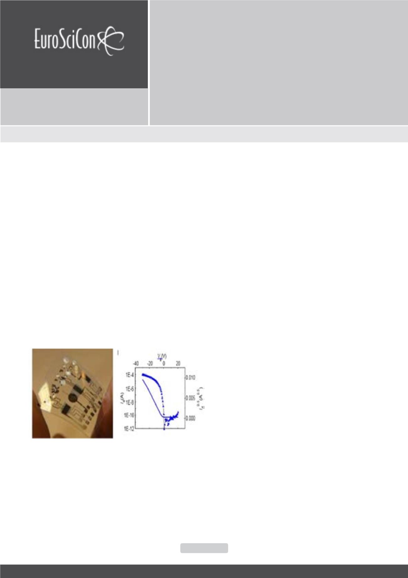
Figure 1:
An array of OTFTand capacitor deviceswith polymer dielectric, and
typical OTFTtransfer curve.