ISSN : ISSN No. 2472-1123
Journal of Organic & Inorganic Chemistry
Effect of surface and interfaces: band gap engineering to achieve high efficiency functional materials and its tunability
2nd Edition of EuroSciCon Conference on Chemistry
February 19-20, 2019 | Prague, Czech Republic
Sudeshna Chattopadhyay
MEMS, BSBE-IIT Indore, India
Posters & Accepted Abstracts: J Org Inorg Chem
DOI: 10.21767/2472-1123-C1-021
Abstract
Controlled thin film coating opens up a promising pathway for band gap engineering and designing the interface mediated defect levels generation, with significant tuneability, which leads to achieving enhanced performance of a given semiconductor in terms of their opto-electronic and electrochemical properties. For e.g., controlled growth of epitaxial graphene (EG) layers on silicon carbide (SiC) provides a novel way of tuning photocatalytic activity and bandgap narrowing in EG/SiC, yielding high efficiency photocatalyst. Results show that the quality and quantity of EG and heterojunction interface layer between EG and SiC, play a crucial role in band gap narrowing, and substantial enhancement of photocatalytic activity in EG/SiC systems. Second example is the atomic layer deposition (ALD) grown ZnO thin films (about 2 nm to 70 nm) on different templates including thin polymeric templates, which formulate a mechanism to achieve significant tunable changes in deep level emission (DLE) of ZnO from green to violet emission range, and in the ratio of DLE to near band edge emission (NBE) from about 0 to 100. The wide range notable variation of photoluminescence and UV-Vis absorption spectra of ZnO are discussed in reference to its potential use as a transparent conducting oxide material and prospective application in ultraviolet light-emitting diodes and solar cell.
Biography
E-mail:
sudeshna@iiti.ac.in
Google Scholar citation report
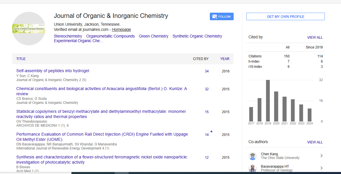
Citations : 150
Journal of Organic & Inorganic Chemistry received 150 citations as per Google Scholar report
Abstracted/Indexed in
- Google Scholar
- China National Knowledge Infrastructure (CNKI)
- Directory of Research Journal Indexing (DRJI)
- WorldCat
- Geneva Foundation for Medical Education and Research
- Secret Search Engine Labs
Open Access Journals
- Aquaculture & Veterinary Science
- Chemistry & Chemical Sciences
- Clinical Sciences
- Engineering
- General Science
- Genetics & Molecular Biology
- Health Care & Nursing
- Immunology & Microbiology
- Materials Science
- Mathematics & Physics
- Medical Sciences
- Neurology & Psychiatry
- Oncology & Cancer Science
- Pharmaceutical Sciences